
The harmful and environmentally damaging chemicals PFAS, short for per- and polyfluoroalkyl substances, are widely used in many industries due to their stability and resistance to water and grease. In the production of semiconductors, for example, membranes containing PFAS are used in numerous process steps. Researchers at the Fraunhofer Institute for Applied Polymer Research IAP have now developed a sustainable alternative in the form of a new type of PFAS-free membrane. The chemically stable, highly permeable polymer membrane has a pore diameter of approx. seven nanometers and enables the filtration of the smallest particle impurities. The membrane can be customized so that the new process can be easily integrated into existing systems.

PFAS chemicals are toxic, they permanently pollute water and soil and accumulate in humans and animals via food and consumer products. In February 2023, the European Chemicals Agency (ECHA) therefore published the proposal for a ban on the manufacture, use and placing on the market, including import, of PFAS in the European Economic Area. The semiconductor industry is critical of the impending PFAS ban, as these chemicals are used in etching and cleaning processes, for example, but also as membranes and housings in filters. According to many manufacturers, there is no alternative to the long-lasting perfluorinated and polyfluorinated chemicals, and the production of most semiconductor products would then no longer be possible. Researchers at the Fraunhofer IAP in Potsdam have now succeeded in developing a PFAS-free membrane made of conventional, specifically stabilized polymers that can replace PFAS membranes for a supplier to the semiconductor industry.
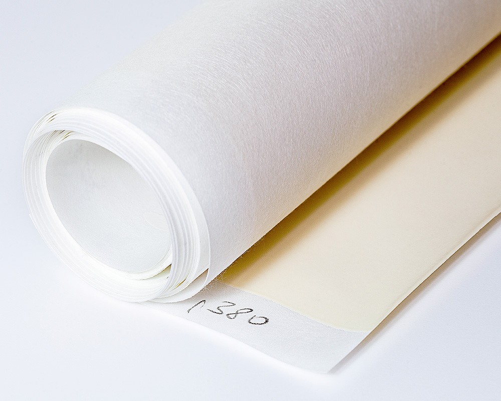
Diaphragm made of PAN
The membrane made of the polymer polyacrylonitrile (PAN) is characterized by high chemical and mechanical stability. It also has an extremely small pore diameter of around seven nanometers. This is necessary to separate particulate impurities from production and to filter and recycle the operating fluids required for the process, such as acids and solvents. The membrane can be customized so that the new process can be easily integrated into existing systems for manufacturing the next generation of chips.
Contamination must be avoided
“When chips are manufactured, countless process steps such as sawing, cleaning and planarization take place in order to apply the structures to the wafers. All of these operations generate particulate impurities that have to be separated during each process, otherwise they would damage the production of the nanometer-sized structures,” explains Dr. Murat Tutus, engineer at the Fraunhofer IAP and head of the“Membranes and Functional Films” department. The team led by Murat Tutus has succeeded in creating a chemically and mechanically highly stable membrane made of conventional polymer that can sieve out particles with a pore size of just seven nanometers. For comparison: In medical technology, filters in the size range of 220 nanometers are used for sterile filtration. “We were able to chemically modify the polymer with another component that we patented and stabilize it for harsh process conditions,” says the researcher.
The researchers were also faced with the task of achieving a pore size distribution that deviated only slightly from the seven nanometers. In addition, the membrane should be highly permeable. “The degree of permeability defines the number of pores on the surface. The smaller the pores, the lower the permeability. In the second step, we therefore had to increase the number of pores while keeping the pore size constant in order to increase the permeability,” explains Tutus.
Production of the membrane with REACH-compliant solvents
As the membrane can be customized via the pore size and permeability, it can be easily adapted to a wide range of applications in other industries. The advantage of adapting a membrane is that existing systems can continue to be used and employees do not need to be trained. Dr. Tutus and his team see great potential for their developments, particularly in the pharmaceutical and chemical industries, where aggressive solvents are also used. Sustainable, REACH-compliant (Registration, Evaluation, Authorization and Restriction of Chemicals) solvents are used in the production of the membrane itself, and the entire production process is designed to be sustainable at low temperatures. The membrane is produced using the NIPS process, short for non-solvent-induced phase separation, whereby the researchers can also adapt the morphology, i.e. the pressure stability of the membrane.
Picture at the top: Novel, PFAS-free high-tech membrane can filter out the smallest particle impurities, enabling the production of next-generation semiconductors. Photo: